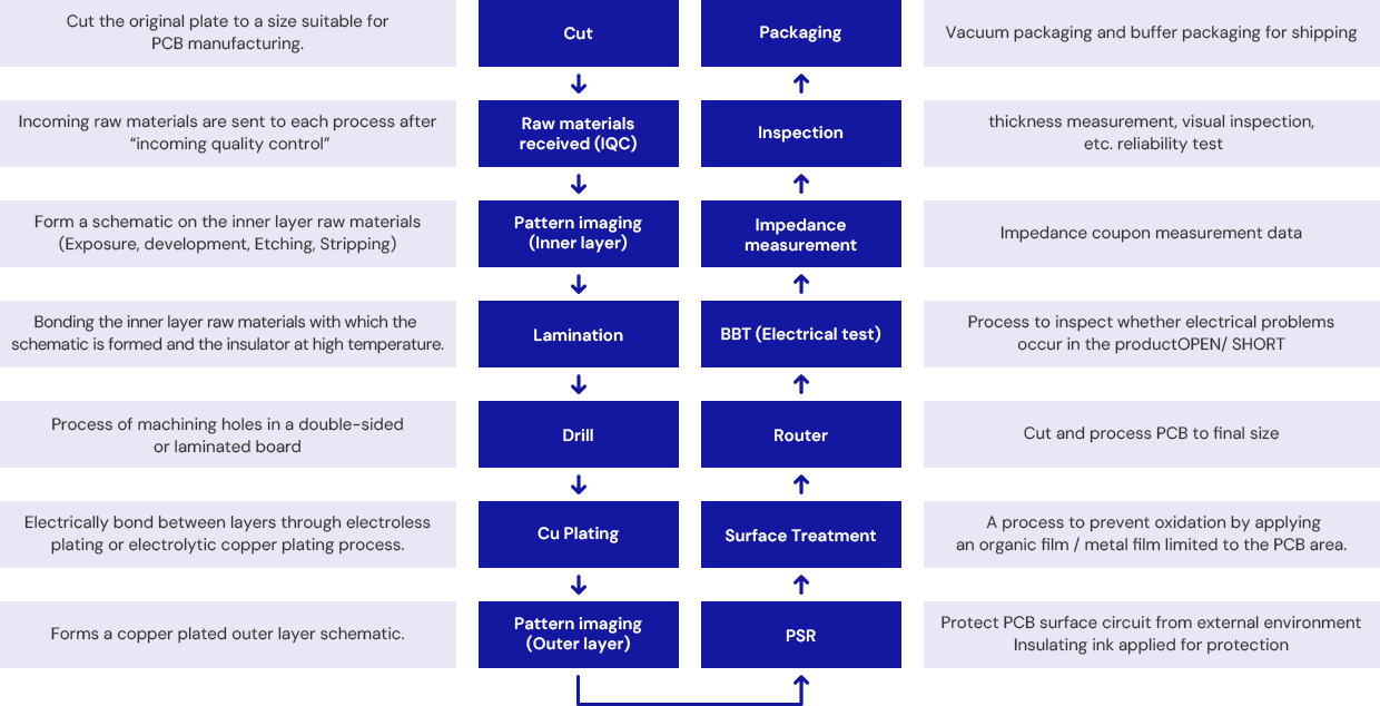
PCB Manufacturing
High Reliability, Excellent Quality, SemiconductorㆍSpecial industrial and Build-up PCB Supply
Semiconductor verification of memory, LSI, ASIC, MPW, etc.ㆍApplicationㆍMountingㆍReliability Test PCB, Substrate Packaging PCB
Automotive ElectronicsㆍDefense industryㆍAviation(Drone)ㆍShip & Ports, etc. Special PCB, electricaㆍelectronic industry
Build-up PCB, Flex PCB, RF-PCB, Impedance PCB, Metal PCB, Ceramic PCB
Supply of 1~70 layer sample PCB and mass production PCB

MTech Manufacturable Capable PCB Specifications
MTech Manufacturing Capable PCB Specifications
| Item | Specifications |
|---|---|
| Layer | 1L~70L |
| Size | 650x600mm |
| Thickness | 0.2mm ~ 6.8mm |
| Pitch | 0.4Pitch(@3.2~3.8mmT) |
| Impedance | ±5 ~ 10% |
| Gold plating Thickness | ENIG/Electro Gold 0.03~1.5um |
| Min Trace Width | 15㎛(Substrate) 50㎛ (Inner Layer) |
| Option | BVH, IVH, HPL, Back Drilling, Build-Up, Substrate |
| Via hole size | Min 0.15 ~ 0.3mm |
| Surface treatment | ENIG / E-less Gold / Electro Gold |
| Item | Specifications |
|---|---|
| Drilled to Copper | 0.1 (DUT Area) 0.15(Other Area) |
| Stacked Microvias | Yes |
| Back Drill | 0.3Pitch |
| Laser Drilled Micro vias | 0.08 ~ 0.1 |
| Blind Mechanical Vias | 0.12 |
| Solder Mask Dam | Min 0.1 |
| Routing tolerance | ±0.1mm |
| External Trace / Space Internal Trace / Space Surbstrate Trace / Space |
0.75 / 0.75 0.050 / 0.050 0.15 / 0.15 |
| Max Panel Siz | 600X780mm |
| PCB material | FR-4, FR-4Hi-Tg, 185HR, N4000-13, N4000-13SI, Epoxy, Composite, Flexible, Teflon, Metal, Isola I-Tera, Polymide, Megatro6~7, DS-7402C, Ceramic |
|---|
- Substrate PCB manufacturing for semiconductor packages
- BGA 0.3mm~0.35mm pitch PCB manufacturing
- Cu 10Oz PCB Manufacturing
Basic Manufacturable PCB Material Specifications
Basic Manufacturable PCB Material Specifications
| Raw materials name | manufacturing company | Material name | Dielectric Constant(Dk) @10GHz (@1GHz) |
Dissipation Factor(Df) @10GHz (@1GHz) |
Tg @DMA | Areas of application |
|---|---|---|---|---|---|---|
| FR-4 High-Tg | EMC | EM-827(I) | (4.3) | (0.019) | 185℃ | Consumer electronics,Automotive, Server & Computer |
| FR-4 Halogen-Free | DOOSAN | DS-7402 | 4.21 (4.33) | 0.014 (0.013) | 165℃ | Smart Device - Mobile, Consumer Electronics Automotive - ECU / DCU / TCU |
| DS-7402LC | 4.1 (4.23) | 0.008 (0.007) | 175℃ | Smart Device - Mobile, Consumer Electronics, Memory module & SSD | ||
| FR-4 High-Tg | DS-7409S(N) | 3.56 (4.3) | 0.019 (0.016) | 190℃ | Networks Equipment - Enterprise/Carrier Router & Switch | |
| DS-7409HG(LE) | 4.1 (4.2) | 0.008 (0.007) | 240℃ | IC Package Substrate- Memory - NAND Flash | ||
| Low CTE BT | MGC(MITSUBISHI GAS CHEMICAL) | HL832NSF (Core) | 3.9(4.0) | 0.006(0.008) | 300℃ | IC Package - Substrate - LSI & Memory - Flip Chip Package, CSP, BGA, etc. |
| GHPL830NSF (PPG & Build-up) | 3.4(3.5) | 0.009(0.007) | 300℃ | |||
| NELCO | AGC INC | N4000-13 | 3.6 (3.7) | 0.009(0.009) | 240℃ | High Speed Semiconductor Test, High-speed storage network, Internet Switch/Routing system, Wireless communication infrastructure, Backplane |
| N4000-13 SI | 3.2 (3.4) | 0.008(0.008) | 240℃ | |||
| I-Tera | Isola | MT40 | 3.45(5GHz) | 0.0031(5GHz) | 230℃ | Medical, Industrial & Instrumentation, Aerospace & Defense, Computing, Storage & Peripherals, Networking & Communication Systems, Automotive & Transportation |
| MEGTRON6 | PANASONIC | R-5775_(Laminate) | 3.39~3.94 (13~56GHz) |
0.0044~0.0072 (13~56GHz) |
210℃ | Gen5 I/F Board, Load Board (SOC Type Mother Board), ICT infrastructure equipment, Measuring instrument, Antenna (Base station, Automotive millimeter-wave radar), Etc |
| R-5670_(Prepreg) | 3.21~3.62 (13~56GHz) |
0.0044~0.0072 (13~56GHz) |
210℃ | |||
| MEGTRON7 | PANASONIC | R-5785N_(Laminate) | 3.11~3.37 (14~59GHz) |
0.0021~0.0033 (14~59GHz) |
210℃ | |
| R-5680N_(Prepreg) | 3.09~3.37 (14~59GHz) |
0.0020~0.0032 (14~59GHz) |
210℃ |
📌 Scroll horizontally to access additional information.
Description of materials available for PCB fabrication
Description of materials available for PCB Manufacturing
| FR-4 | The substrate characteristics of multiple layers of glass fiber impregnated with epoxy resin meet most electrical and physical needs and can be applied to most products. |
|---|---|
| FR-4 Hi-Tg | Substrate with higher Tg than FR-4. Glass transition temperature of 170ºC, improved heat resistance |
| N4000-13 SI | Low Permittivity, Excellent price / Performance is good |
| Epoxy | A substrate made by synthesizing and laminating epoxy resin on glass fiber. It has excellent electrical properties, excellent dimensional stability, and excellent heat and chemical resistance. |
| Composite | A substrate made by synthesizing and stacking two or more materials. You can combine them to suit your desired characteristics. |
| Flexible | Copper foil is coated on polyester or polyimide film for excellent insulation and heat resistance and free design |
| Teflon | High-frequency PCB design using Teflon as an insulator, easy impedance adjustment, excellent electrical stability and heat resistance |
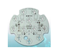
| METAL | This is a board made by anodizing an aluminum plate capable of high frequency and high heat dissipation and then bonding copper foil to it. |
| Polyimide | A substrate made by laminating polyimide film and copper foil without using adhesives. Excellent bending strength and flexibility, excellent thermal stability, and excellent abrasion resistance. |
| Isola I-Tera | It is a material suitable for high-speed digital and RF/microwave applications and has stable electrical characteristics over a wide frequency and temperature range. |
| Megatro6 | A high-speed, low-loss multi-layer material designed for high-speed network equipment, mainframes, IC testers, and high-frequency measurement devices. |
| DS-7402C | Higher thermal properties than existing lead-free FR-4 (above 170℃), excellent chemical and heat resistance, UV blocking and AOI compatibility, Build-Up PCB Material |
| Ceramic | We can supply a variety of ceramic PCBs, including DCB boards made from alumina (AI2O3) and aluminum nitride (AIN). Compared to general PCB boards, it has high thermal conductivity, excellent dielectric properties, high electrical insulation strength, stable chemical properties, strong corrosion resistance, and excellent reliability under high temperature and high pressure conditions, so it is mainly used for power industry, home appliances, industrial use, defense and aerospace, automotive, medical, etc. Applies. |
PCB type
PCB Type
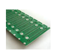
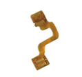
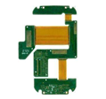
| Single Side | Double Side | Multy Layer | Impedance | FPCB | Rigid FPCB | Metal | Package Substrate | Ceramic |
|---|---|---|---|---|---|---|---|---|
 |
 |
 |
 |
 |
 |
 |
 |
 |
|
|
|
|
|
|
|
|
|
📌 Scroll horizontally to access additional information.
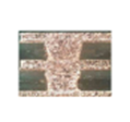
Via hole processing
Via hole Processing
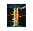
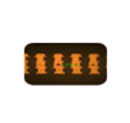
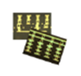
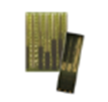
| PTH | HPL | IVH | BVH | Build-up | Back Drilling | Stack-Via |
|---|---|---|---|---|---|---|
 |
 |
 |
 |
 |
 |
 |
|
|
|
|
|
|
|
| Plated Through Hole | Hole Plugging Land | Interstitial Via Hole | Blind Via Hole | Micro Via Drill | Stub Length Specification 250um±125um |
📌 Scroll horizontally to access additional information.
 tel. +82-31-548-0212
 email. mtech@mtechpcb.co.kr

