Semiconductor Packaging
Semiconductor Packaging, C.O.B (Chip on Board)
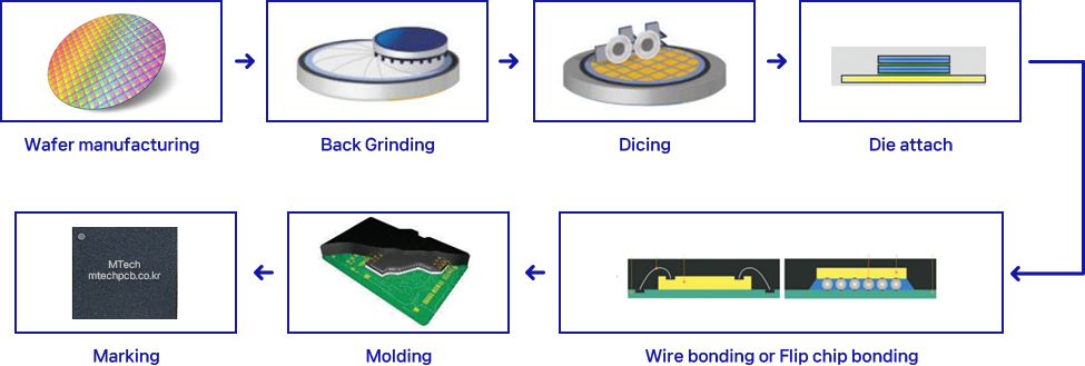
We provide customized package services such as Flip Chip, CSP, BGA, etc. Package, Prototype Package, COB, etc. in cooperation with domestic and foreign OSAT companies.

Package Sample Assembly Capability
Package Sample Assembly Capability
LF Mold Type
| QFN |
|---|
 |
|
Open Cavity Package
| QFN | LQFP | DFN | SOIC |
|---|---|---|---|
 |
 |
 |
 |
|
|
|
|
📌 Scroll horizontally to access additional information.
Other Package
| Ceramic | CLCC | PGA | FPGA |
|---|---|---|---|
 |
 |
 |
 |
| Supports all FPGAs that customers want |
📌 Scroll horizontally to access additional information.
Other Package
| COB(CHIP ON BOARD) |
|---|
 |
| Wire Bonder Capability K&S maxum ultra fine pad pitch up to 45um |
MLPGA Package Substrate
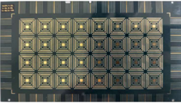
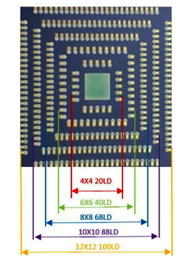
MLPGA (Multi Land Plastic Grid Array) Package Substrate
| MLPGA Substrate | |
|---|---|
 |
A versatile general purpose semiconductor package substrate designed to produce packages of various sizes, lead counts and shapes desired by customers using a single substrate. |
Available package : Refer to page 10 ~ 13
|
|
Information required when requesting packaging
Information required when requesting packaging
| Wafer | Die | Package | etc. |
|---|---|---|---|
| 1) Wafer Size Diameter (mm) 2) Incoming Thickness (um) 3) Number of Dies |
1) Die Size (width x height um) 2) PAD Size (width x height um) 3) Number of PADs (left, right, top, bottom) 4) Center distance between the nearest PADs (um) 5) Die PAD shape (inline & staggered mixed) |
1) Package Type 2) Package Size (Width x Height mm) 3) BGA Ball Count 4) BGA Pitch & Ball Size (mm) 5) Solder Ball Material |
1) Substrate layer count, thickness (mm) 2) Die PAD List & Ball Map 3) Bonding Wire material, thickness (mm) 4) Expected number of bonding wires 5) Number of sockets manufactured (Sockets for connection between evaluation board and chip) 6) Whether back grinding and sawing are performed 7) Laser marking details 8) Marking for confirming die location on wafer (whether pencil number marking is performed) |
📌 Scroll horizontally to access additional information.
Package Assembly Mass Production Support
Package Assembly Mass Production Support
- Domestic Ass’y Site Support PKG: FBGA, PBGA, FC FBGA, LGA, QFP, WLCSP, Wafer Bumping (Gold, Solder, Cu Pillar)
- Overseas Ass’y Site Support PKG: BGA, QFP, QFN, SOP, TSSOP, LGA, DIP, SOT, etc.
- Wafer Back Grinding & SAW Outsourcing Support (6” 8” 12”Inch, MPW Wafer included)
- Chip Sorting (GEL PACK or Waffle PACK) possible
Other Package Service
Other Package Services
- Wire Bonding Diagram Spec Production
- Package Substrate PCB Design & PCB Production
- Laser Marking : Package New Marking & Remarking & Partial Marking
- Test Socket Production
- Wafer Probe Test, Final Test
- T&R Packing In House Support
- PKG Defect Analysis Support Service (X-RAY, DECAP, PHOTO, etc.)
 tel. +82-31-548-0212
 email. mtech@mtechpcb.co.kr


